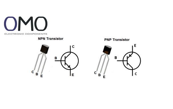
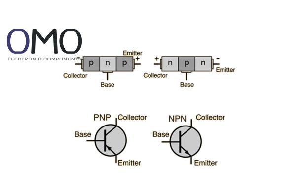
An NPN transistor is a Bipolar Junction Transistor (BJT). It has three layers of semiconductor material. It is one of the most common devices in electronic circuits. It can work as an amplifier or a switch. A small current at the base controls a large current at the collector. The name "NPN" shows the doping order: two N-type layers with one P-type layer in between.
Structure
The NPN transistor has this structure:
Emitter: Heavily doped N-type area. It sends electrons to the base.
Base: Very thin and lightly doped P-type area. It controls the flow of electrons.
Collector: Larger and moderately doped N-type area. It collects electrons.
Electrons are the main carriers of current. Because electrons move faster than holes, NPN transistors usually have higher speed and better frequency response.
Features
Main features of NPN transistors:
Current flow is by electrons. This makes response faster.
More common in digital circuits because of faster switching.
Needs positive voltage at the base (compared to the emitter) to turn on.
Easy to use in low-side switching, where the load is connected to ground.
What is a PNP Transistor?
Basic Concept
A PNP transistor is another type of BJT. Its structure is the opposite of NPN. It has two P-type layers and one N-type layer. It can also amplify signals or act as a switch. The base current controls the collector current, but the voltage polarity and current direction are opposite to NPN.
Structure
The PNP transistor has this structure:
Emitter: Heavily doped P-type area. It sends holes.
Base: Very thin and lightly doped N-type area. It controls the flow of holes.
Collector: Larger and moderately doped P-type area. It collects holes.
Holes are the main carriers. They move slower than electrons. So, PNP transistors are usually a little slower than NPN ones.
Features
Main features of PNP transistors:
Current flow is by holes.
Needs negative voltage (or lower voltage compared to the emitter) at the base to turn on.
Works well in high-side switching, with load connected to ground.
Often used together with NPN transistors in complementary circuits (such as Class B amplifiers).
How Do NPN and PNP Transistors Work?
General Modes
Both types work with the principle of carrier injection and collection. A small base current controls a large collector current. They have three modes:
Cutoff: Base-Emitter (BE) junction not forward biased. No collector current.
Active (Amplification): BE junction forward biased, Base-Collector (BC) junction reverse biased. Collector current is proportional to base current.
Saturation: Both BE and BC junctions forward biased. Collector current is maximum. Transistor is fully on.
NPN Operation
When BE junction is forward biased (Vbe > 0.7V) and BC junction is reverse biased, electrons move from emitter into the base. Because the base is thin and lightly doped, most electrons go to the collector. This creates collector current (Ic). The base current (Ib) controls Ic. Current gain β = Ic / Ib.
PNP Operation
When BE junction is forward biased in the opposite way (Veb > 0.7V, base voltage lower than emitter), and BC junction is forward biased, holes move from emitter into base. Most holes pass through the base and reach the collector. The base current controls collector current, but the voltage polarity is opposite to NPN.
Main Differences Between NPN and PNP
Current Direction
NPN: Current enters collector and leaves emitter (base current flows in).
PNP: Current enters emitter and leaves collector (base current flows out).
Voltage Polarity
NPN: Needs positive base voltage (compared to emitter). Collector usually has the highest voltage.
PNP: Needs negative (or lower) base voltage. Emitter usually has the highest voltage.
Symbol
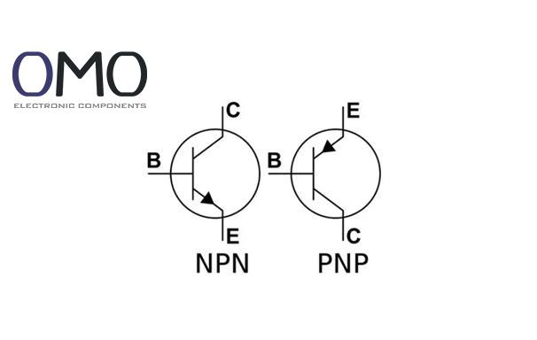
NPN: Arrow on emitter points out.
PNP: Arrow on emitter points in.
Main Carriers
NPN: Electrons (faster).
PNP: Holes (slower).
Comparison Table:
Feature
NPN Transistor
PNP Transistor
Current direction
Collector → Emitter
Emitter → Collector
Base drive voltage
Positive (to emitter)
Negative (to emitter)
Symbol arrow
Outward
Inward
Main carriers
Electrons
Holes
Typical use
Low-side switch, digital circuits
High-side switch, complementary circuits
Applications of NPN and PNP Transistors
NPN Applications
NPN transistors are fast and easy to use. Common uses:
Switch Mode Power Supply (SMPS): High-frequency switching for better efficiency.
Digital logic circuits (like TTL): As fast switches.
High-frequency amplifiers and oscillators: For RF communication and signal processing.
Sensor interface circuits: Example: amplify or switch signals from optical sensors.
PNP Applications
PNP transistors are useful in:
Complementary push-pull stage: Together with NPN in Class B amplifiers, reduces distortion.
High-side switch: Drives load connected to ground, simple design.
Linear regulators: Works as pass transistor, gives stable voltage output.
Pull-up elements: As load or current source with NPN circuits.
Pros and Cons
NPN Transistor
Pros:
High electron mobility → faster switching and higher frequency.
Many models available, lower cost.
Easy in low-side switch circuits.
Cons:
Needs complex base drive in high-side switch use.
May need extra protection in high-voltage circuits.
PNP Transistor
Pros:
Good for high-side switching. Load can connect directly to ground.
Important in complementary designs.
Easier in some linear circuits.
Cons:
Lower mobility of holes → slower response.
Fewer models, sometimes higher cost.
Can NPN and PNP Be Exchanged?
Direct Exchange
No, they cannot be directly exchanged. Voltage polarity and current direction are opposite. Direct replacement will stop the circuit or damage parts.
How to Replace Function
If replacement is needed, you must redesign the circuit:
Reverse the power supply polarity.
Change direction of polarized components (capacitors, diodes).
Adjust bias resistors to match new voltage and current.
So, designers must choose NPN or PNP at the start.
Key Parameters
Common Parameters
Important parameters for both types:
Current gain (hFE / β): Ratio of Ic to Ib, usually 50–800.
Collector-Emitter breakdown voltage (Vceo): Max voltage with base open, usually 30–1000 V.
Collector current (Ic): Max continuous collector current, usually 100 mA–10 A.
Power dissipation (Pc): Max collector power, needs heat sink.
Transition frequency (fT): Frequency when gain = 1. Shows speed. NPN usually higher.
NPN vs PNP Parameters
Even with same type of parameter, values can differ. For example, in complementary pairs, NPN often has 20–30% higher fT.
2N3904 (NPN) vs 2N3906 (PNP):
Parameter
2N3904(NPN)
2N3906(PNP)
Vceo
40 V
40 V
Ic (max)
200 mA
200 mA
hFE (typical)
100
100
fT
300 MHz
250 MHz
Pc
625 mW
625 mW
Frequently Asked Questions
When to use pnp and npn transistor?
PNP transistors are suited for high-side switching or controlling negative voltages, while NPN transistors are used for low-side switching or positive voltage control.
How do you bias a PNP transistor?
To ensure proper operation, the base-emitter junction must be forward-biased and the base-collector junction must be reverse-biased. This is achieved by applying a positive voltage to the emitter while using negative voltages for both the base and collector.
How do NPN and PNP transistors switch current?
An NPN transistor allows current to flow from the collector to the emitter when a small base current is applied. Conversely, a PNP transistor permits current to flow from the emitter to the collector when the base current is removed.
How can you distinguish between NPN and PNP transistors by using a multimeter?
When testing a transistor in diode mode:For an NPN type, place the red probe on the base and the black probe on either the emitter or collector.For a PNP type, place the black probe on the base and the red probe on the emitter or collector.